
Indie game storeFree gamesFun gamesHorror games
Game developmentAssetsComics
SalesBundles
Jobs
TagsGame Engines

Digital Logic Sim

​A minimalistic digital logic simulator · By Sebastian Lague

Working CPU

A topic by sam0x56 created 71 days ago Views: 468 Replies: 10
Viewing posts 1 to 4
(+2)

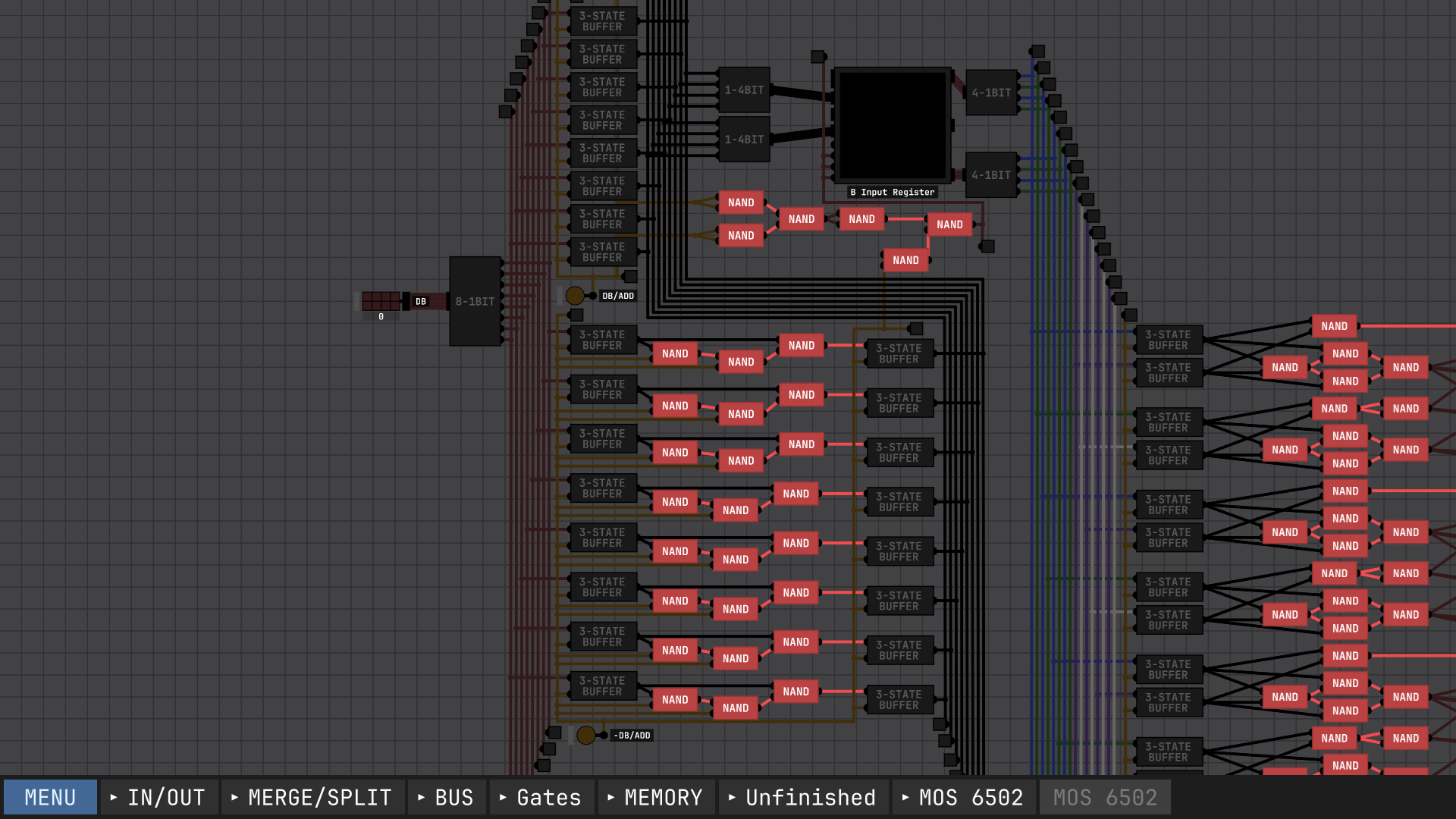
I started following along with Sebastian's videos but then I got carried away and made a working CPU based on Simple As Possible (SAP) CPU architecture.  

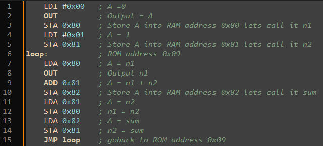
I got it to work. in the video, it is doing Fibonacci series(up to 255 then things go weird for obvious reasons, I do have the key R bound to reset the CPU which I press a few times in the video if you wondered)


Some details about the architecture: 

It only supports the following few instructions :

  • NOP = (1 byte) No operation - OpCode = 0x00
  • LDA = (2 bytes) Load Reg A (form Memory Address) - OpCode = 0x01
  • ADD = (2 bytes) Add Value of memory address to A and stores it in A - OpCode = 0x02
  • SUB = (2 bytes) Subtracts Value of memory address to A and stores it in A - OpCode = 0x03
  • STA = (2 bytes) Stores Reg A into Memory Address - OpCode = 0x04
  • LDI = (2 bytes) Load Reg A immediate value - OpCode = 0x05
  • JMP = (2 bytes) JMP to address - OpCode = 0x06
  • JC = (2 bytes) Jump if Carry to address - OpCode = 0x07
  • JZ = (2 bytes) Jump if Zero (flag) to address - OpCode = 0x08
  • OUT = (1 byte) loads whatever in A into the output register (therefore display) - OpCode = 0x0E
  • HLT = (1 byte) Halts the program - OpCode = 0x0F

Addressing space is split only between RAM and ROM as follows:

  • ROM address space is 0x00 to 0x7F (128bytes)
  • RAM address space is 0x80 to 0xFF (128bytes)

the program it's running in the video can be represented as the screenshot below, which is stored in ROM as hex values directly, of course.


Here is the save file if you want it https://drive.google.com/file/d/1R2pp46HE2XlyOyXfhV24VUoxapS8Anuj/view

It should work on version 2.14. you can extract the save file here: %localappdata%\..\LocalLow\SebastianLague\Digital-Logic-Sim\Projects (if you are on windows)

Disclaimers: 

  • download and use at your own risk.
  • It is not the most stable thing. could be a bug from the simulator itself or something off with the design. but it does take a few reloading the save file to get it to run smoothly and in a stable way. 
  • the save file includes some saved chips that are not used in this.  SAP is the one that has the working implementation.

Key binds:

  • R = Resets the counters
  • S = Synchronizes (rests) all display settings. useful when using multiple display modules in the same chip and you want them to all have the same settings.
  • T = Toggle between signed and unsigned 7seg displays
  • B = turn on/off blanking on the 7seg displays 

oh wow, good job! Also, it's assembly part looks really close to mine, i could help you make an actual assembler in c++

thank you :) it was fun to make with this sim. a few years ago I stumbled upon this https://github.com/hlorenzi/customasm. easy to use for any custom assembly you want. I Incorporated it in yet another SAP implementation I made using C# https://github.com/SamFarah/SAP1-Emulator/tree/SAP2 

(1 edit)

oh wow, that's really cool! I didn't know customasm is a thing and just made my own assembler, that would've been waaay easier...

(+1)

but can it run doom?

Sadly , not yet

lol, i wish

But first You must optimize your current logic for example You use a lot of XOR / EOR , but if I good remember you made it from 2 not one AND and 3 other gate but You can make it use only 4 NAND , less gates = quicker simulation , and one more the simulation see user use a special gate for example AND gate so simulation must stop and load AND gate simulate them back to current simulation, but if you use NAND the simulation don`t must stop because you will use basic brick

correct. it has huge room for optimization. I've even seen people use the dot display as RAM, I could have utilized that because the RAM chip is the main component that heavily affects performance. but I was aiming mostly for a conceptual and intuitive design rather than an optimized one 

XD I understood You , now I almost done ALU in mos6502 but I use only NAND some times looks like a pasta , BUT WORK as well XP
About RAM Use RGB 8pin for address and 2x4 bit for data (more data in one place ) and if you use only data without address You will got a register ( Load pin conect to save refresh and clock , Read use 2 4to1 bit and use 8 3state buffer)


(2 edits)

Question: how do you access the RAM? I see you've use the top bit of the address to toggle between ROM and RAM, but can you input that bit in the code?

If the instruction takes the top four bits, then the address can only be the bottom four. That makes only 16 memory locations total.

I'm running into the same issue on my system and I'm considering adding control line to select either RAM or ROM. (though it would still be limited to 16 locations each).