
Indie game storeFree gamesFun gamesHorror games
Game developmentAssetsComics
SalesBundles
Jobs
TagsGame Engines

Digital Logic Sim

​A minimalistic digital logic simulator · By Sebastian Lague

Multi-Purpose 4-Digit Numeric Display

A topic by gardrek created 48 days ago Views: 270 Replies: 11
Viewing posts 1 to 8
(+1)

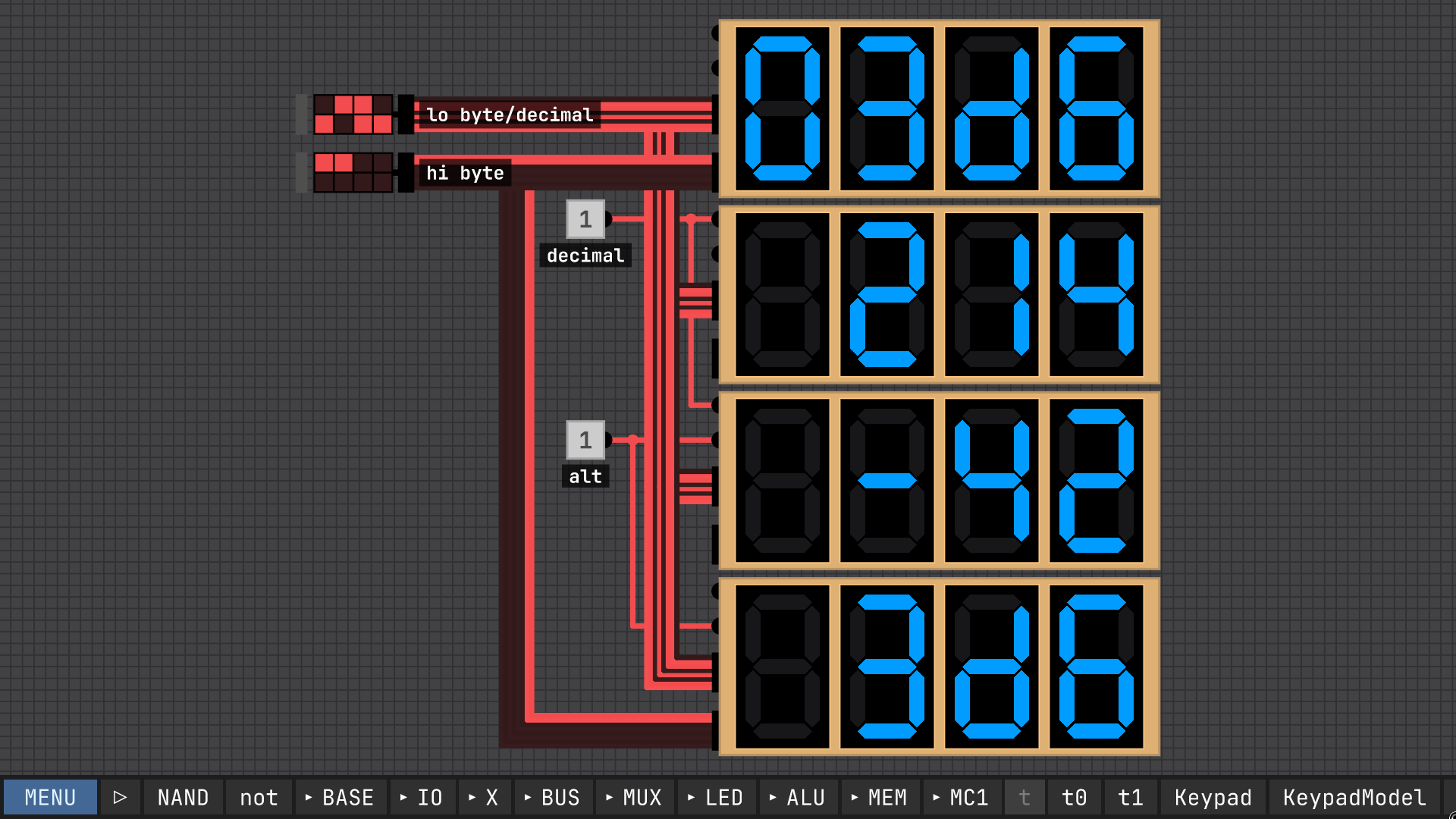
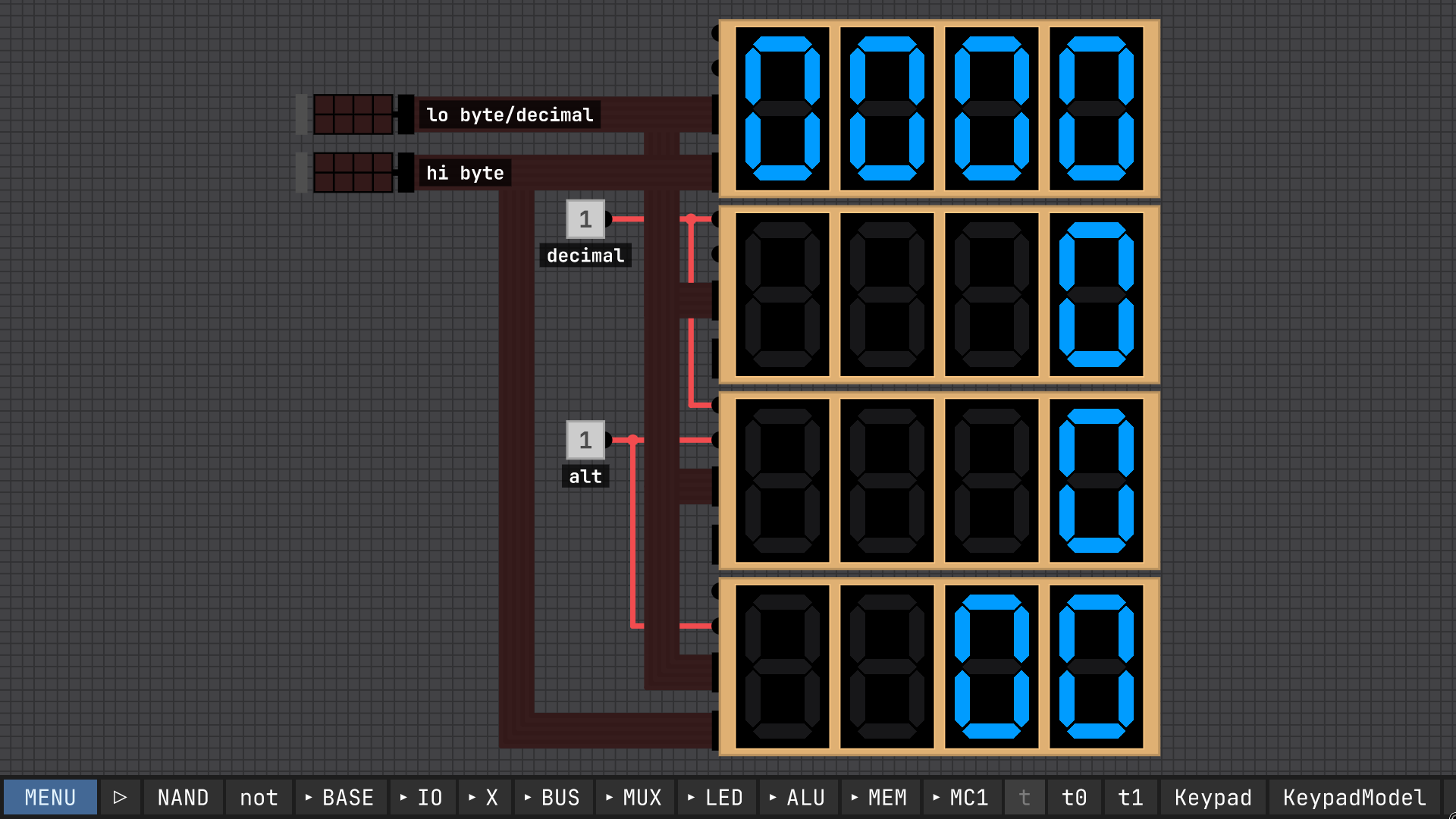
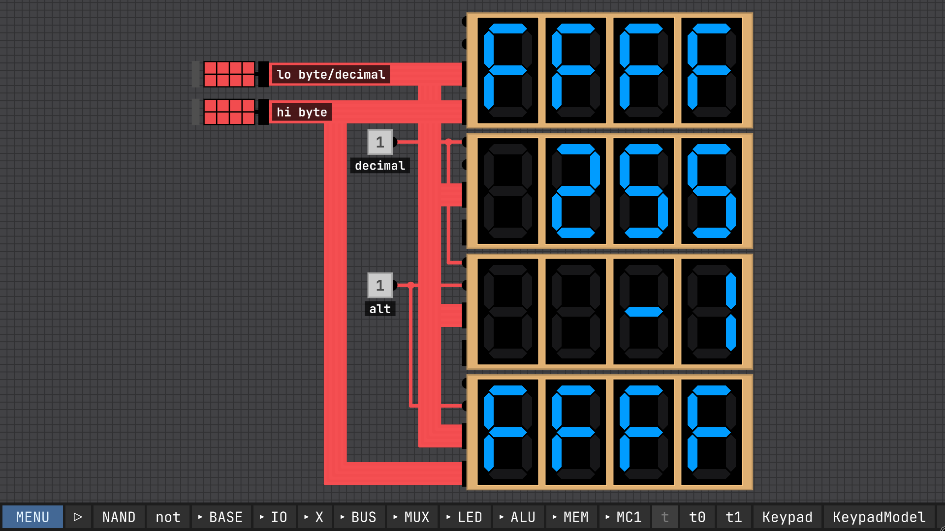
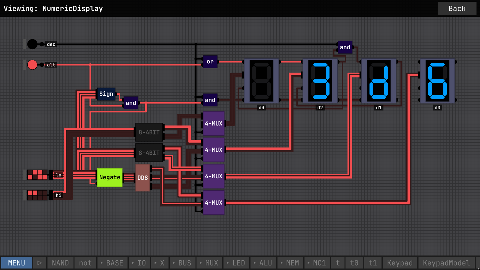
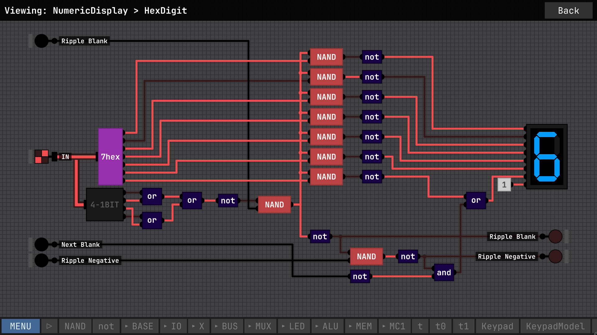
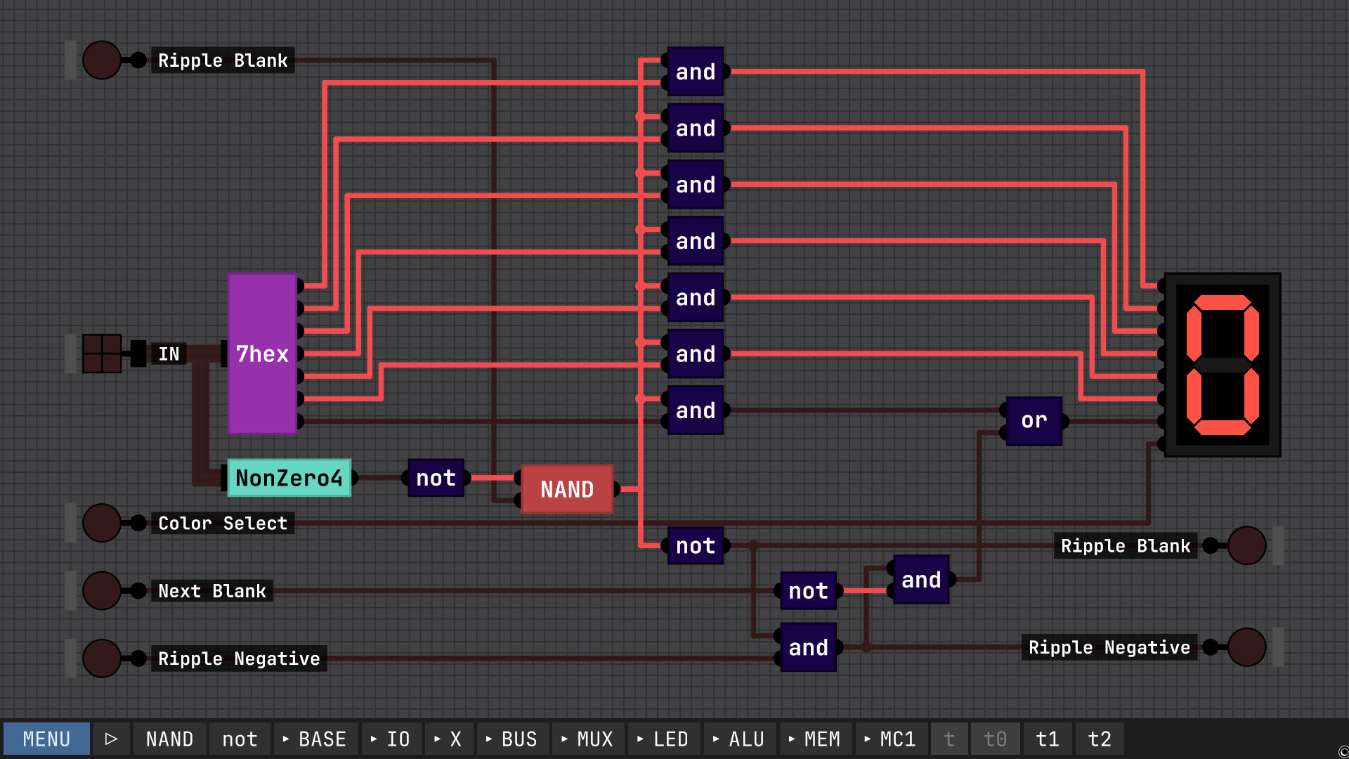
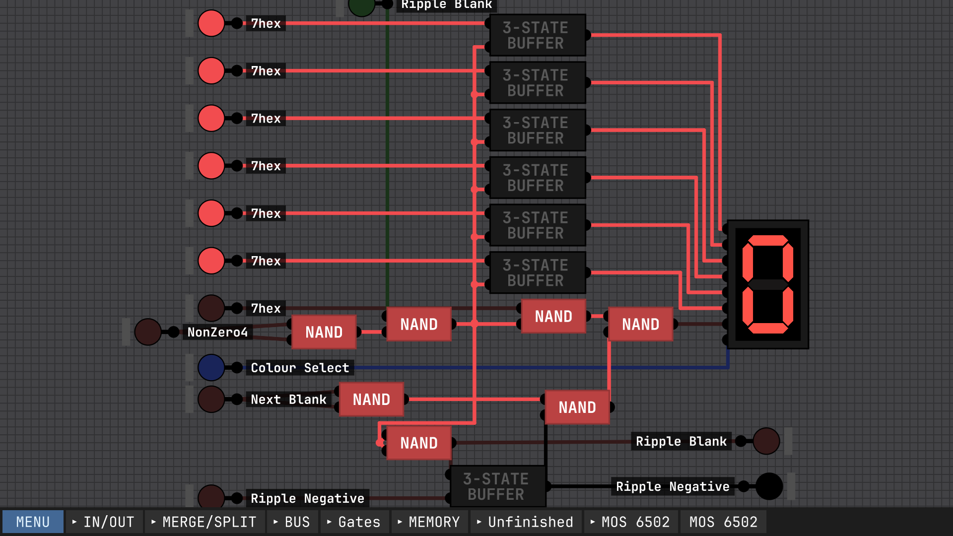
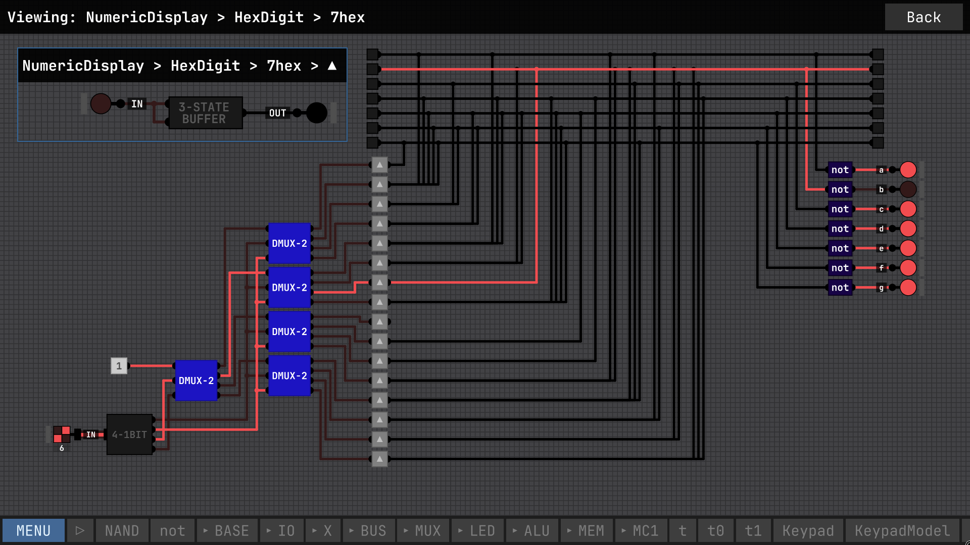
I created this numeric display following along with the videos and tweaking things, along with developing my own design for a bus-based seven-segment encoder. It has four modes: (top to bottom in the screenshots) four-digit hexadecimal, unsigned decimal, signed decimal, and the last mode being hexadecimal with zero blanking for the first 2 digits, so it will display a single byte padded with a leading zero, but display the upper byte with blanking. Note that all multi-bit inputs are LSB at the top, in other words little-endian in reading order, the opposite of the convention used in the videos the numeric display built in to IO pins.


If you change OR gate (near 1) to NAND You will not need extra NOT gate (+ must change And to NAND {second connection to OR for correct logic}) always one less gate ^^

Ah, I see what you mean. I already redesigned this though. I do like to optimize for minimal NAND gates but I also like to aim for clarity too, so it's a balance.

the new layout: 

OK , but why don`t eat a cake , and have a cake XD
I made based on your screenshot optimize version , maybe I will inspire You =P
I will hope You like it ^^

Interesting use of tri-state buffers. Good if you're going for absolute optimization of gate numbers. Actually, in the context of the rest of the circuit you could possibly take it even further, by using active-low inputs for the ripple signals. and maybe even removing the inverters on the display ROM.

I'll try to explain my design and reasoning, working up from the seven-segment encoder. The "7hex" chip uses a demultiplexer with the input tied high simply because I did not  build a dedicated decoder at that point yet. Using such a decoder would save a lot of NANDs so I will probably switch to that. From there the signals go into a series of three-state buffers with the enable tied to the data, turning the signals into "three-state bits" if you will. These are tied to one bus per output line, making essentially an easy to program ROM by tying each input to the buses corresponding to a "one" in that position. The busses are then inverted, because inverting this output meant drawing less ROM lines (i.e. the average output pattern has more ones than zeroes).

Moving on to the "Hex Digit" module, it is set up pretty similarly to the display in the videos, with the ripple blanking checking if the digit is zero AND if ripple blanking is in, then blanking this digit and sending ripple blank out. The ripple negative was more complicated tho. The only solution I could come up with was to tie the blanking *output* of the *next* digit back into this one, to "look ahead" to see if we're on the last blank digit, and if so, enable the negative sign.

Finally, the display itself, basically it uses a multiplexer to choose between the decimal and hex formats, and then there's a bit of logic for the hex blanking mode. Other than that it's wired up pretty much as you'd expect, with the blanking wrapping around to the previous digit for the ones that need ripple negative.

Oh yeah, so the chip named DD8 is pretty much exactly the same Double Dabble chip from the videos. Any questions, let me know

Developer

Really nice work! Would be cool to have a video of it in action for the community playlist, if that’s something you’re up for doing :)

(+1)

I am planning to do a video showing all my most interesting circuits, but the scope of the video has increased a bit. I am actually writing a generic assembler that can be programmed to work for any hobby CPU architecture. Because I didn't want to hand assemble a longer MC1 program for the video. By reusing code I already wrote, the assembler is already not far from a usable state, at which point I'll start working on a video.