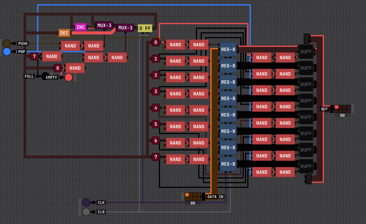
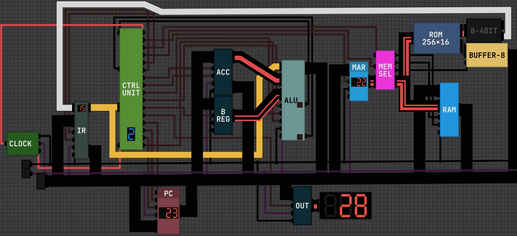
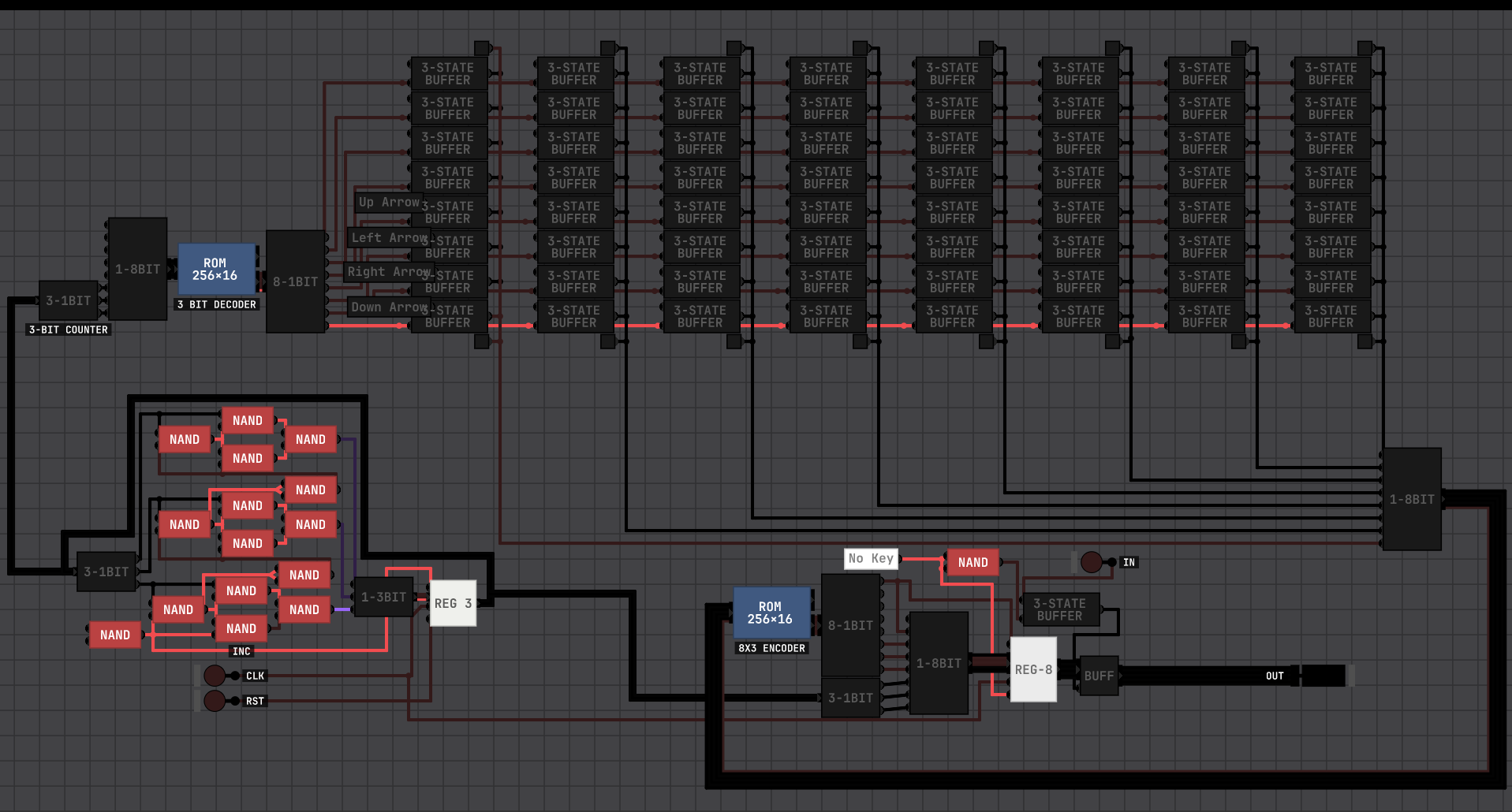
IT HAS R0-R7 GENERAL PURPOSE REG AND 5 GRAPHICS REG (X, Y, R, G AND B).
IT CAN HAVE UP TO 128 INST SET.
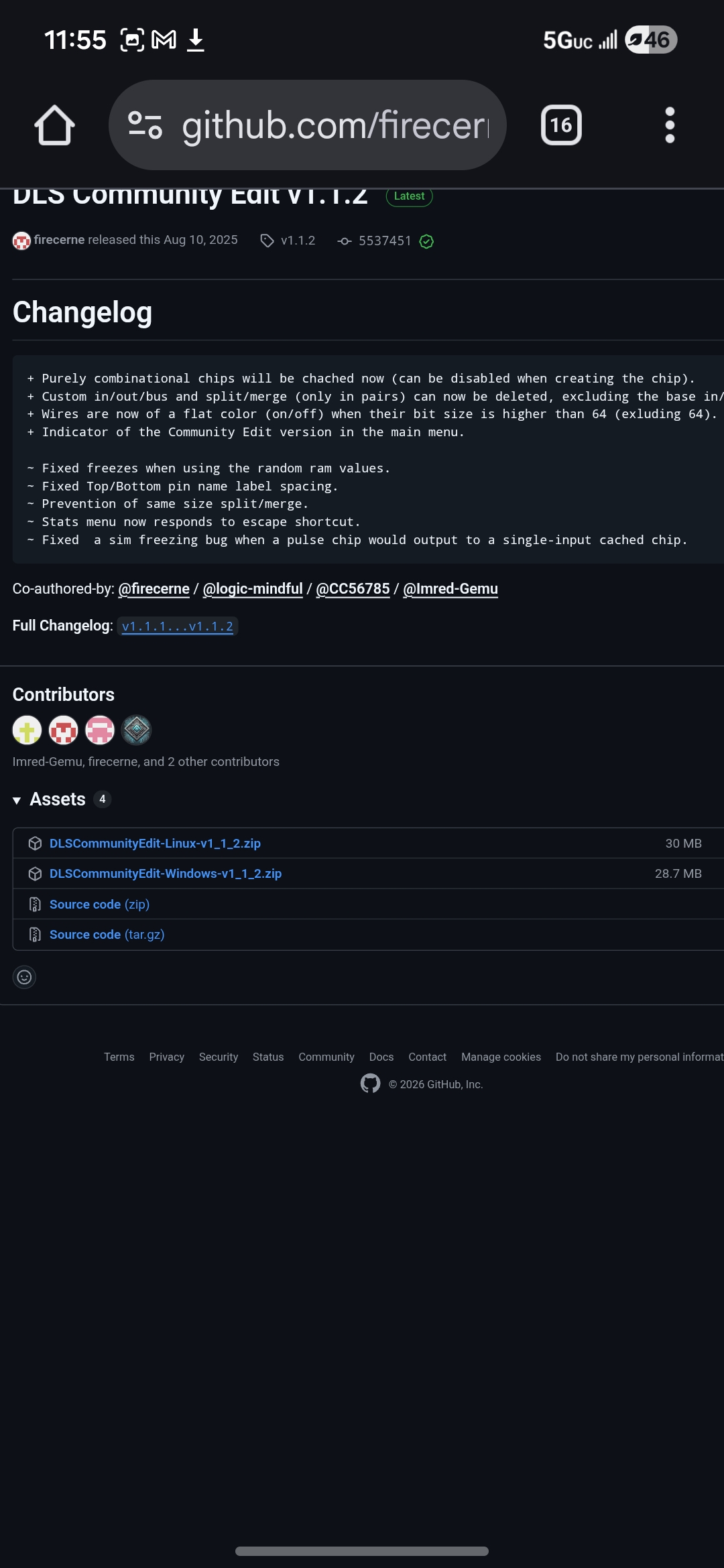
YOU MUST USE THIS DLS 2 VERSION: Release DLS Community Edit v1.2.1 · firecerne/Digital-Logic-Sim-Community-Edit.
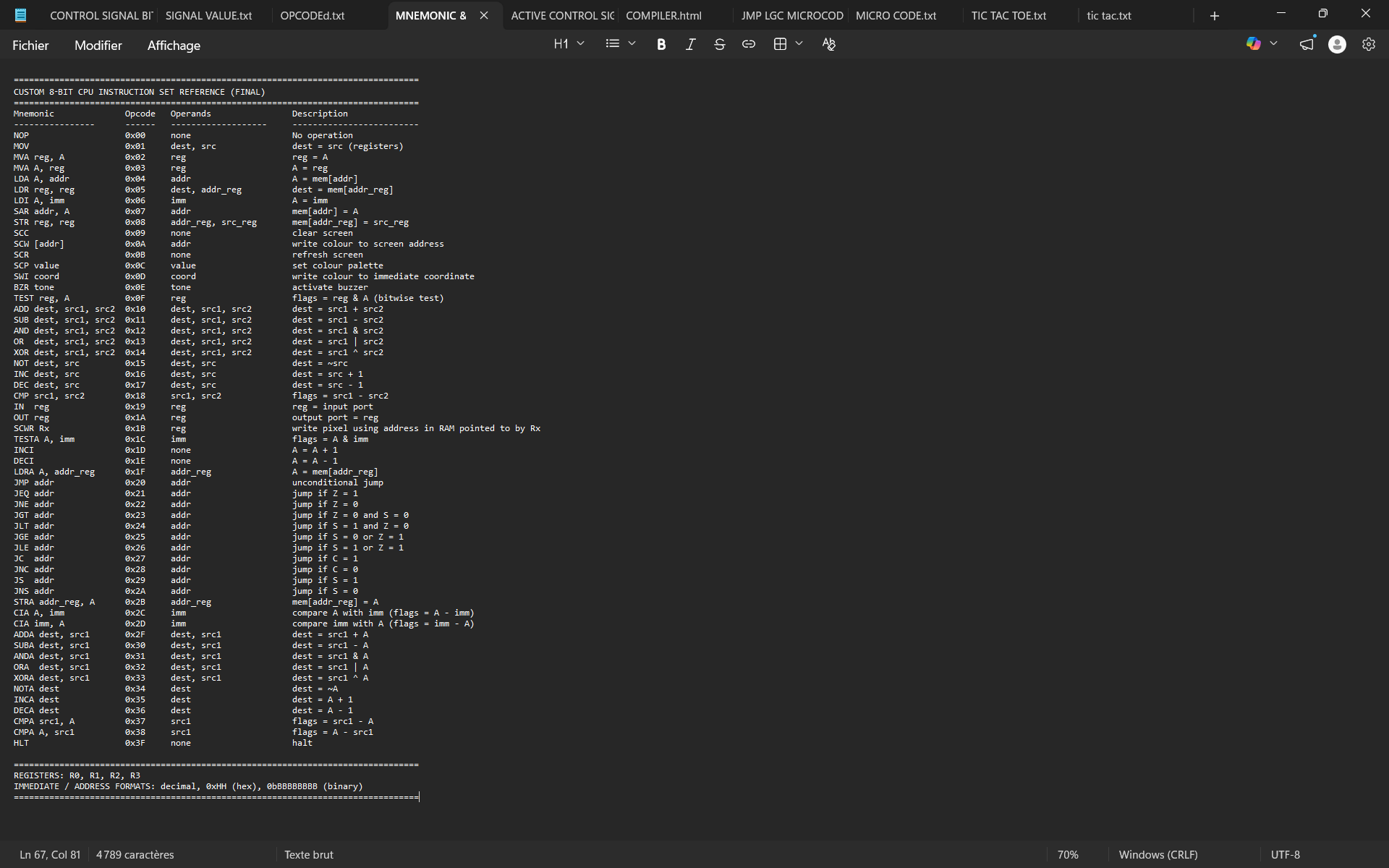
---------------------------------- ALU_OP ENCODING -----------------------------
0000 : ADD 0001 : SUB 0010 : AND 0011 : OR
0100 : XOR 0101 : NOT 0110 : INC 0111 : DEC
1000 : MUL 1001 : DIV 1010 : MOD 1011 : SHL
1100 : SHR 1101 : ROL 1110 : ROR 1111 : NEG
SHL/SHR/ROL/ROR: 0-7
================================================================================
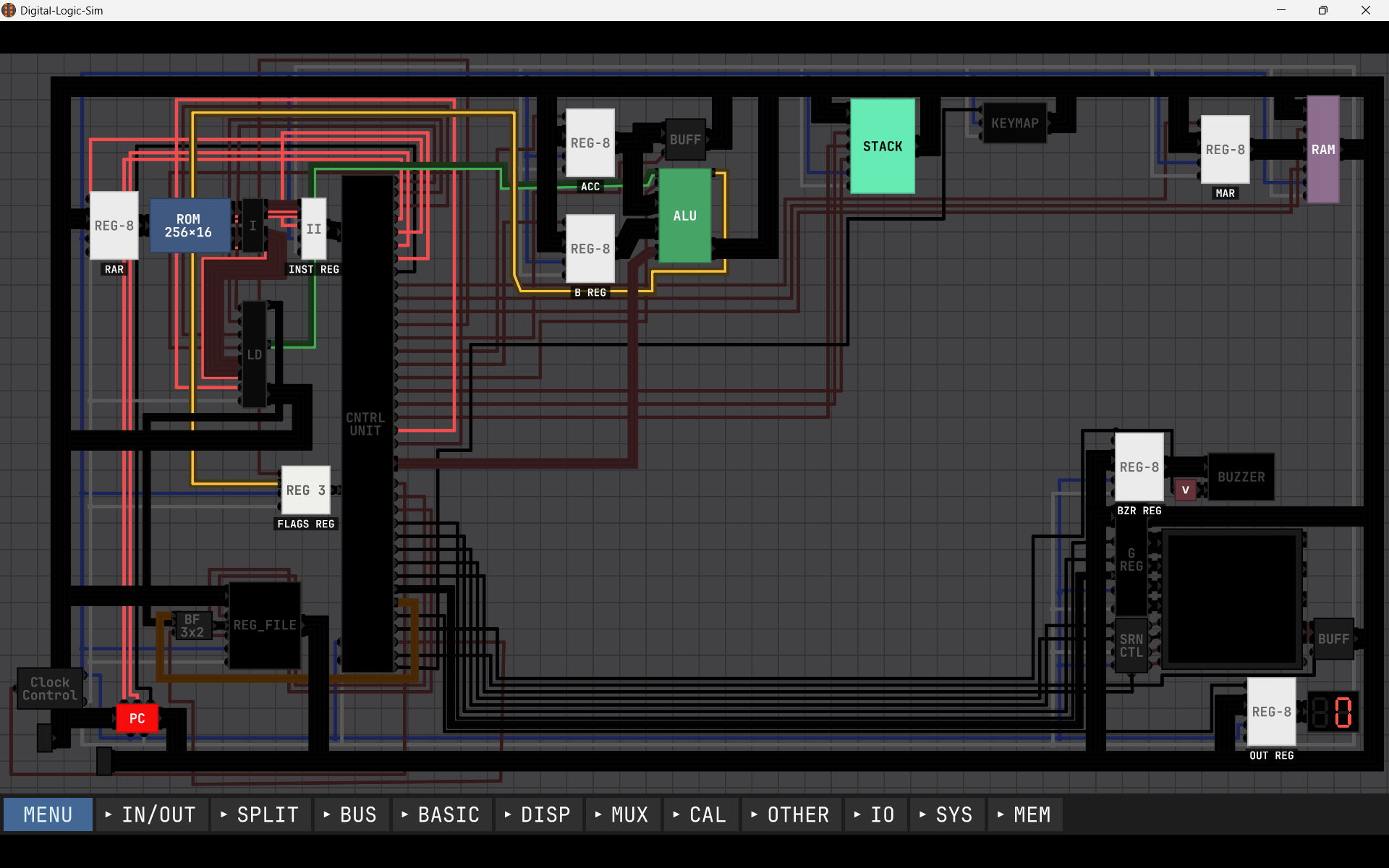
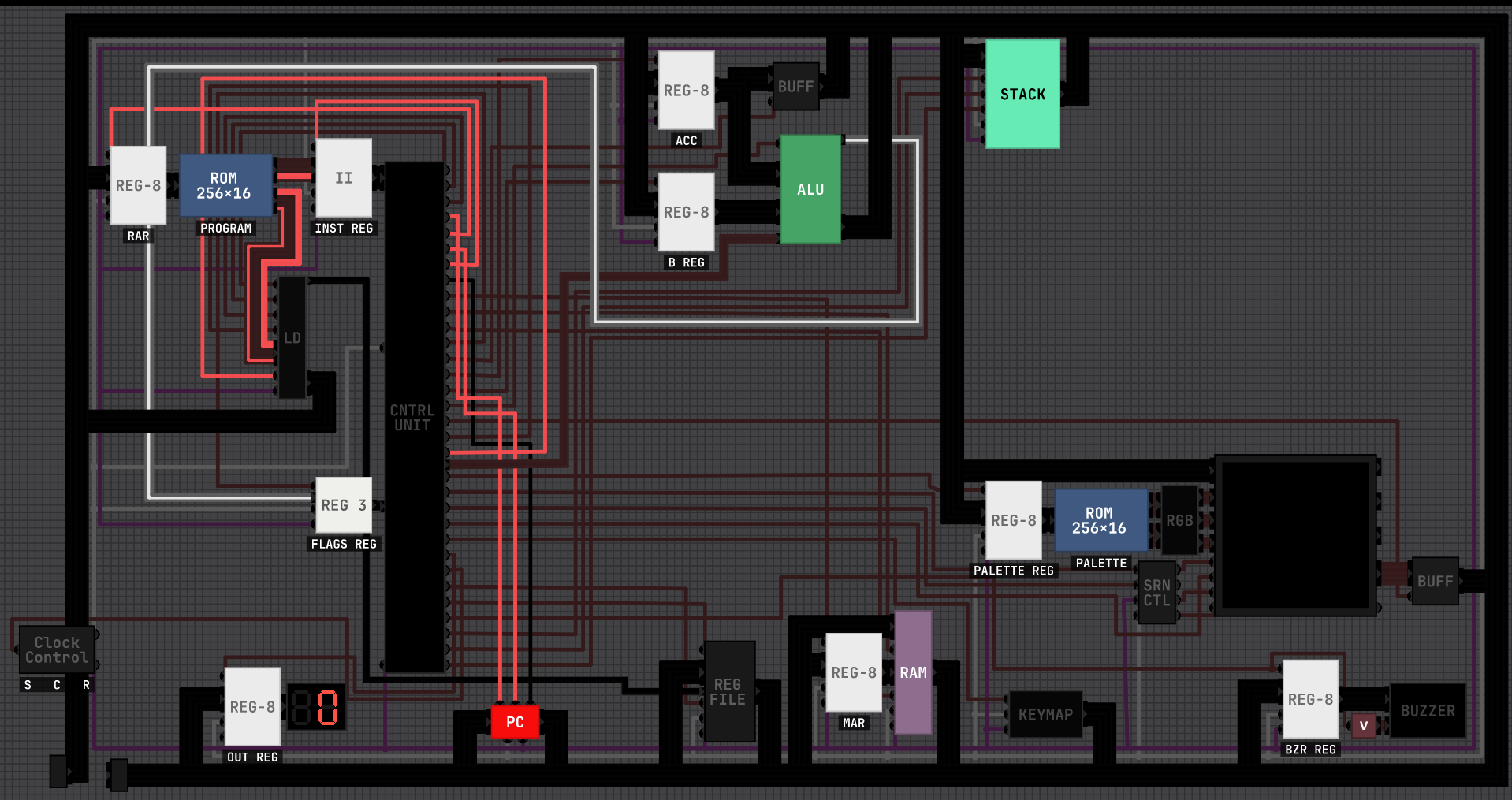
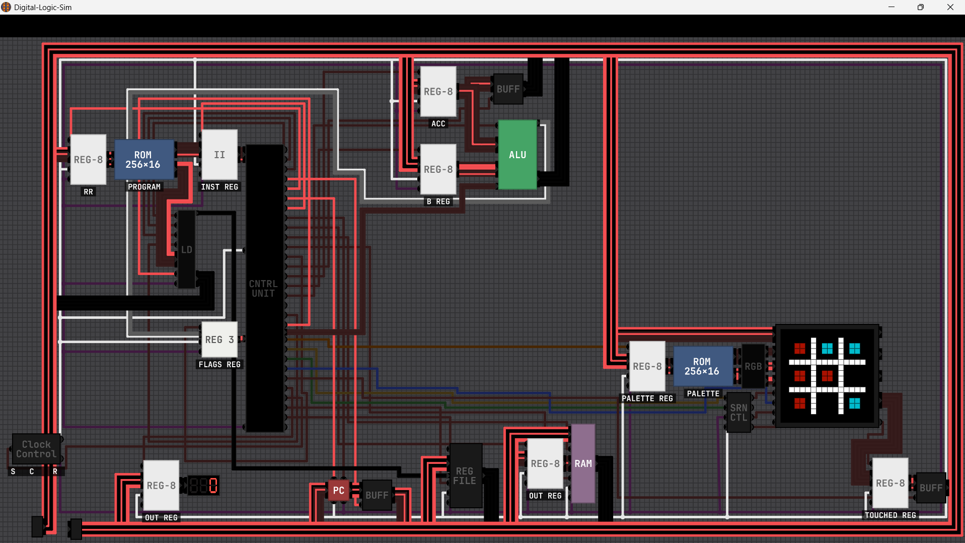
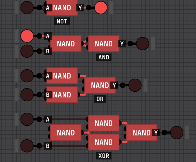
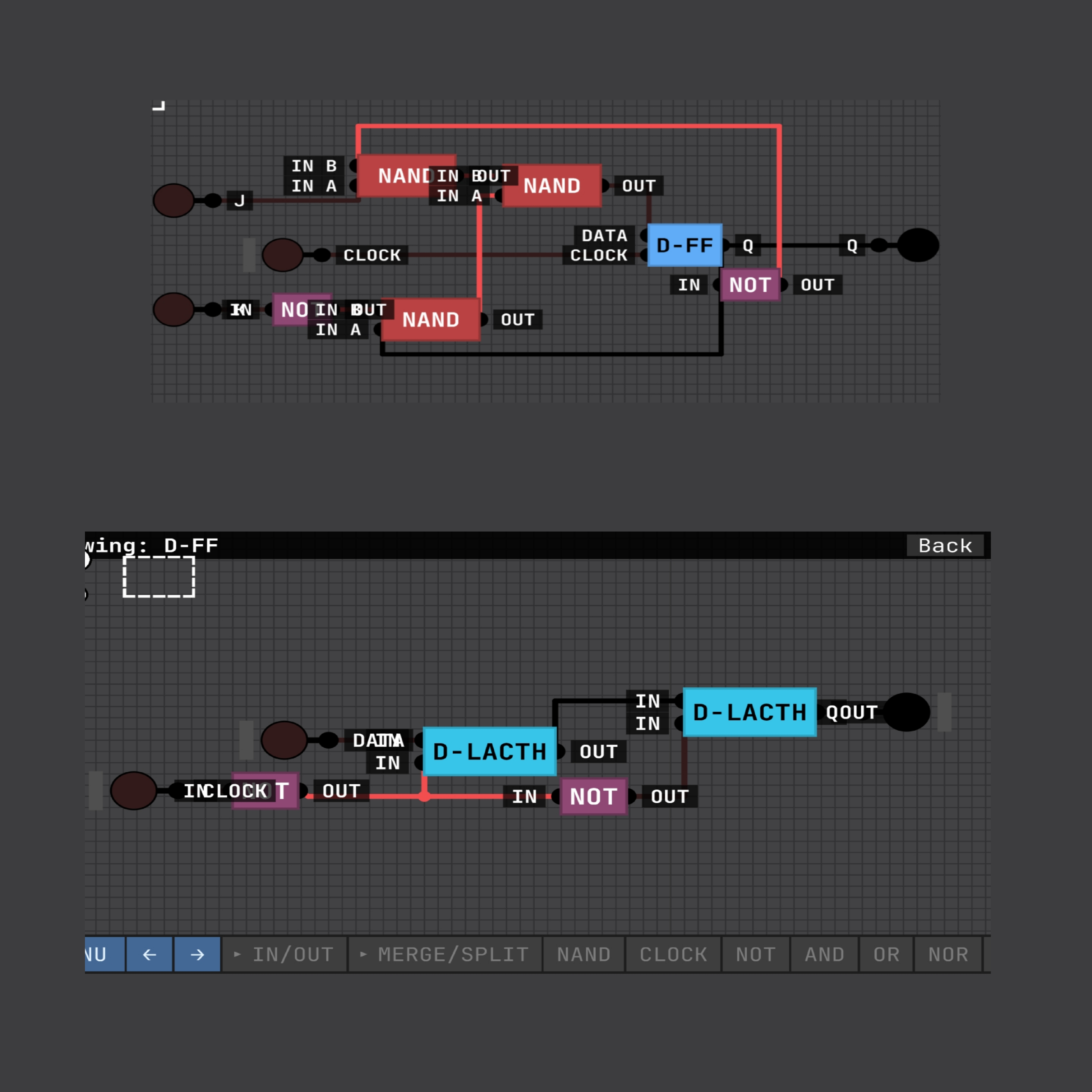
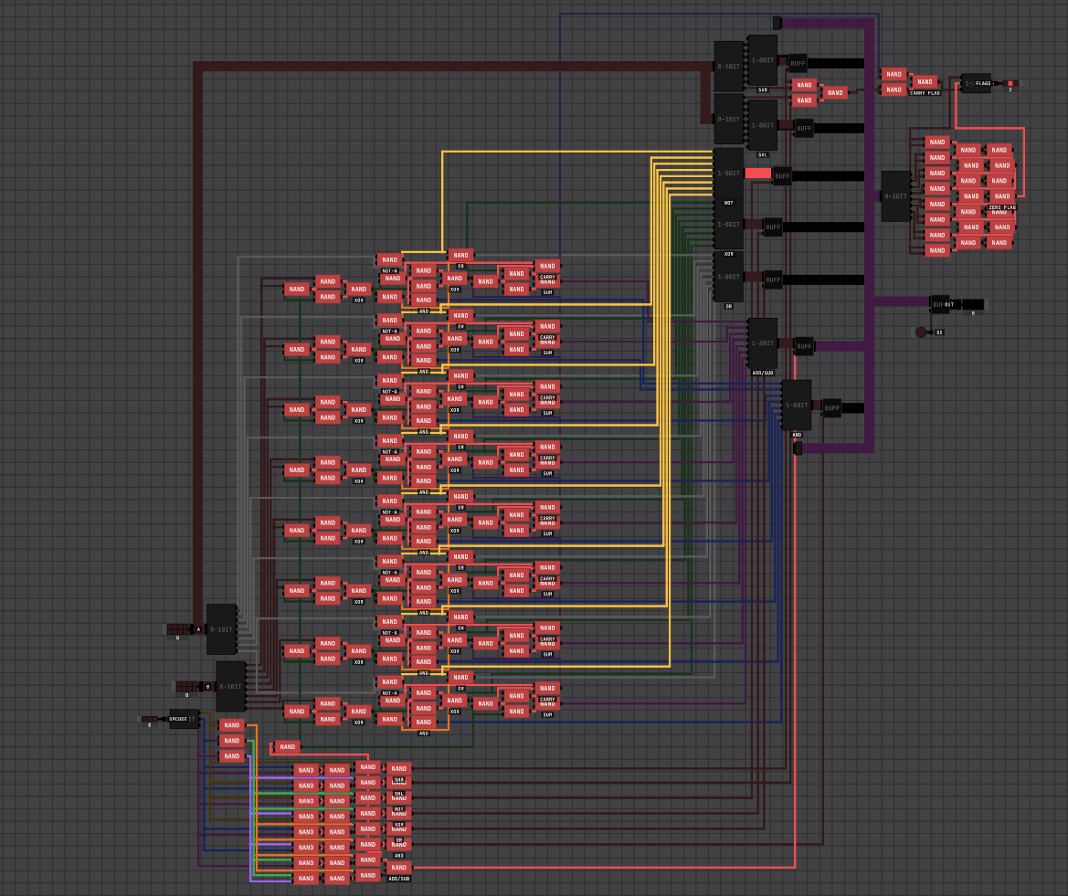 That's a 3-bit op ALU(add/sub, bitwise operation and shift) and three flags.
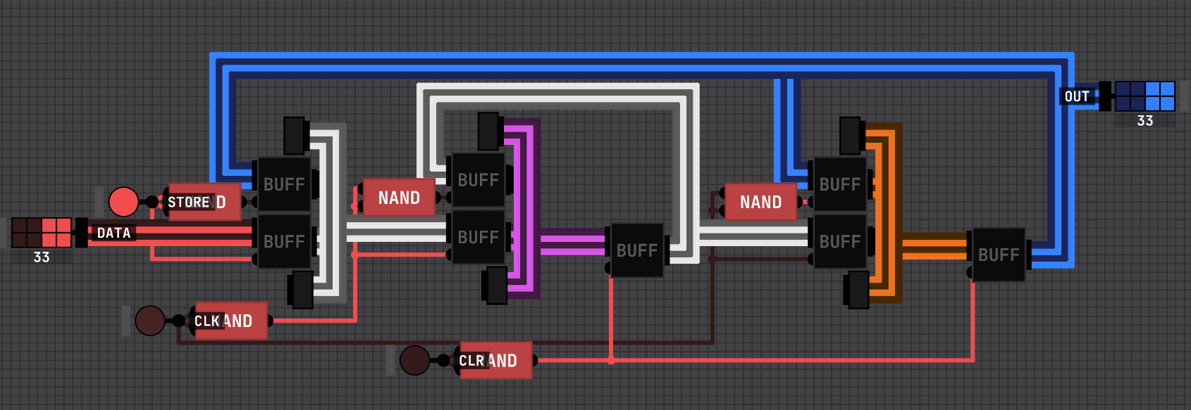 That's an 8-bits reg faster than the old ways.
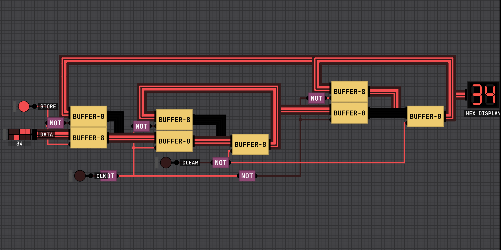